PCB Üretim
27 Şubat 2026
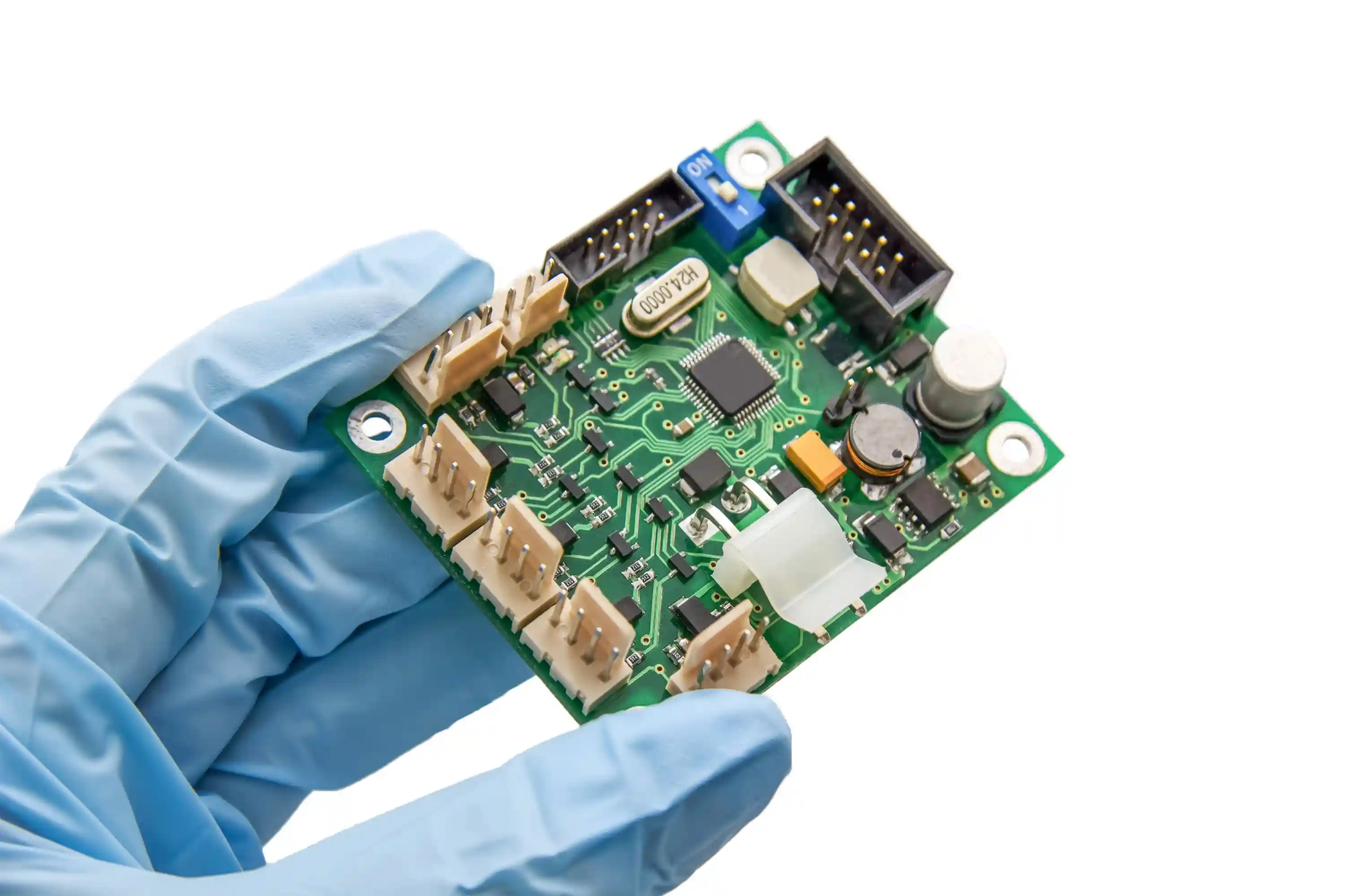
Gerber Dosyası Hazırlama Rehberi: PCB Üretimi İçin Eksiksiz Kılavuz
Gerber dosyalarını doğru şekilde hazırlamayı öğrenin. Dosya formatları, katman yapısı, dışa aktarma adımları, doğrulama kontrol listesi ve en sık yapılan 10 hatayı keşfedin.
Devamını Oku